4-Bit Processor
Digital Logic · TTL · Breadboard · 2025
Introduction
Recently, I built a 4-bit processor. For reference, a 4-bit processor is a CPU designed to process 4 bits of data at a time. It's able to perform operations similar to the ones done by a simple handheld calculator.
Getting Started
I started with a simple indicator circuit. I built this using an inverter chip (74LS06), 330Ω resistors, and LEDs. My set up looked like the following:
Indicator Circuit
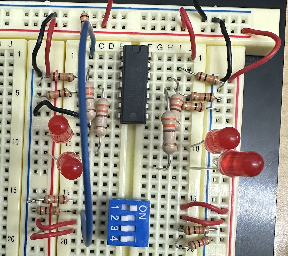
When the input (pin 1) is wired to 0 V, the output of the inverter will be a logic 1, and the LED won't light. But when logic 1 is applied to the input, the output transistor will conduct current and the current limiting resistor will turn the LED on. This basic circuit was used in the future for me to visually confirm outputs (light being on/off).
Background
After setting up this basic indicator circuit, I got to work familiarizing myself with different logic gates. I messed around with a NAND chip (74LS00) and created a NOT, AND, NOR, and 3-Input AND gate from just the NAND chip. Most of the chips used later in this project are internally built from logic gates like the ones I built.
My next step after working with basic gates was moving on to building a selector. The selector picks between different input signals and only sends one to the output based on a separate control signal. This was useful because it allowed me to choose between different data sources depending on a set condition, rather than having my project hardwired to a single condition.
My Design Process
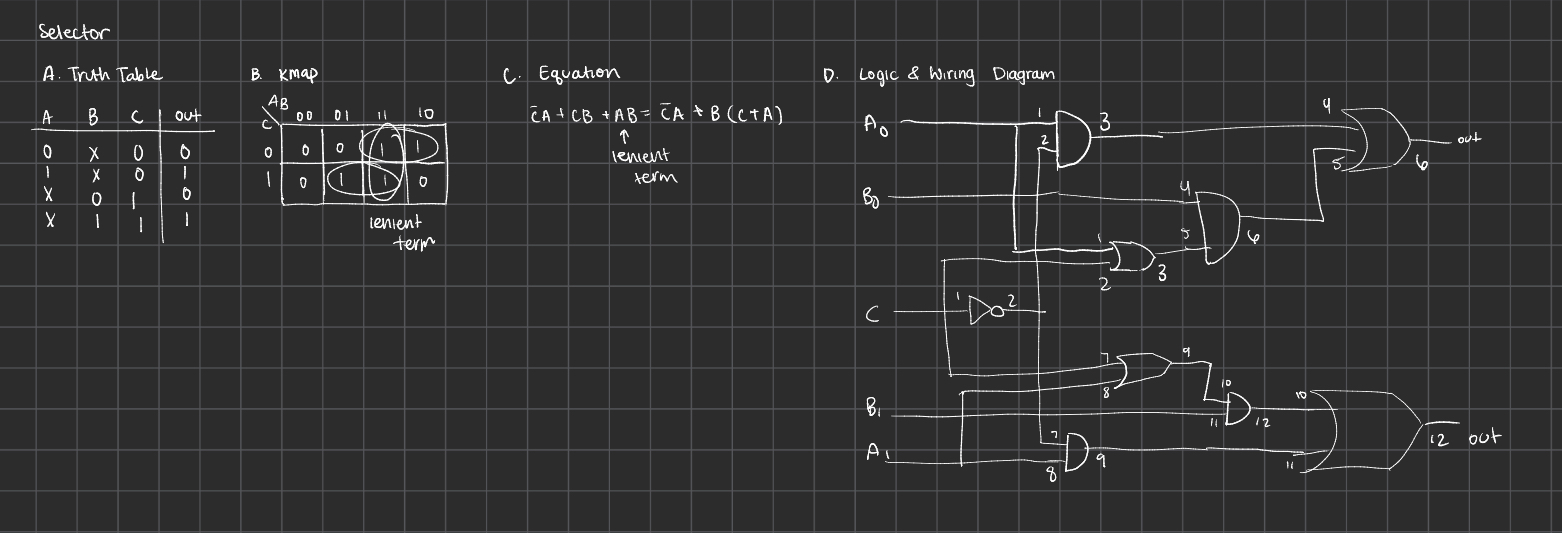
I designed the 1-bit selector with two data inputs, (A and B), one control input (SEL), and one output (Y). Ideally, when SEL was 0, Y should equal A, and when SEL is 1, Y should equal B. I was able to build this using an inverter, two AND gates, and an OR gate, which were wired together as Y = (NOT SEL AND A) OR (SEL AND B). Each of these gates was one that I'd built before using the NAND gate, so I went ahead and used the actual chips 74LS04 (NOT), 74LS08 (AND), and 74LS32 (OR).
Both the AND gates are always computing something at all times, but SEL forces one of the two terms to 0. When SEL is 0, the inverter flips it to 1 and passes A through. So, it outputs an A because 1 AND A = A. The second AND gate sees that SEL is 0, so it computes 0 and B, which is always 0 regardless of the logic value of B. Then, I OR'd these two results together because 0 from B's side won't change anything, so Y just outputs A.
When SEL = 1, it flips the other way. The inverter turns SEL into 0 for the first AND gate, which means the value of A is irrelevant. The second AND gate now sees SEL as 1 and passes B straight through. Then Y becomes equal to B. I connected A and B to switches, and SEL to the third switch, with Y going to an LED indicator circuit. I confirmed the output follows the logic, which means that only SEL determines which LED was lit up.
So, just like that, I'd completed a 1-bit selector. After this, I moved on to creating a 2-bit selector. Instead of a single bit A and B, there were 2-bit inputs A0/A1 and B0/B1, with outputs Y0 and Y1. There was not really any new logic involved in this step. It was just two 1-bit selectors sitting side by side, both wired to the same SEL line.
Selector — Truth Table, K-Map & Wiring
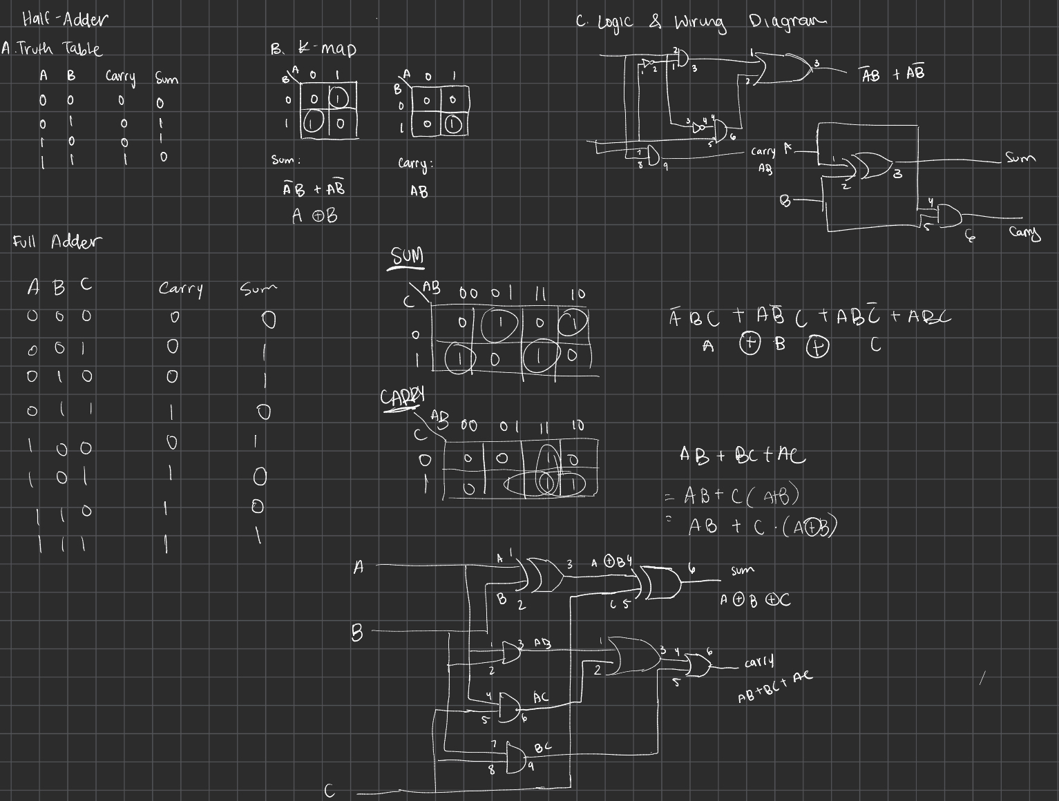
Now that I had created the selector, I got to work making a half adder and eventually a full adder. I started with the simplest case, which was just adding two single bits, A and B. You can see the truth table below! It was a simple XOR logic gate with the carry out representing the sum when the result was too big to fit in one bit.
The half adder worked fine for adding two single bits in isolation, but there was no way to accept a carry that was created by a previous column, and so I couldn't do arithmetic that required two 4-bit numbers. So, I created a full adder, which solved this problem by adding a third input (carry in), alongside A and B. Now there are three inputs and still two outputs: sum and carry out. The truth table got a little bit bigger, which you can also see below.
Half Adder & Full Adder
Sequential Logic
Now, the fun stuff. Up to this point, everything I'd built was combinatorial. Basically, the output depended only on current inputs and changed instantly as inputs changed, with zero memory of the past. The selector and adders are really good examples because once you change A and B, Y immediately changes with it. Sequential logic is a little bit different because a sequential circuit's output depends on both current inputs and a circuit's history. This is the first introduction to memory that I had, and it was a really cool experience!
I started by cross-coupling two NAND gates. Each gate's output fed into one of the other gate's inputs, which formed a loop. The two external inputs are called reset and set, and the single output is Q.
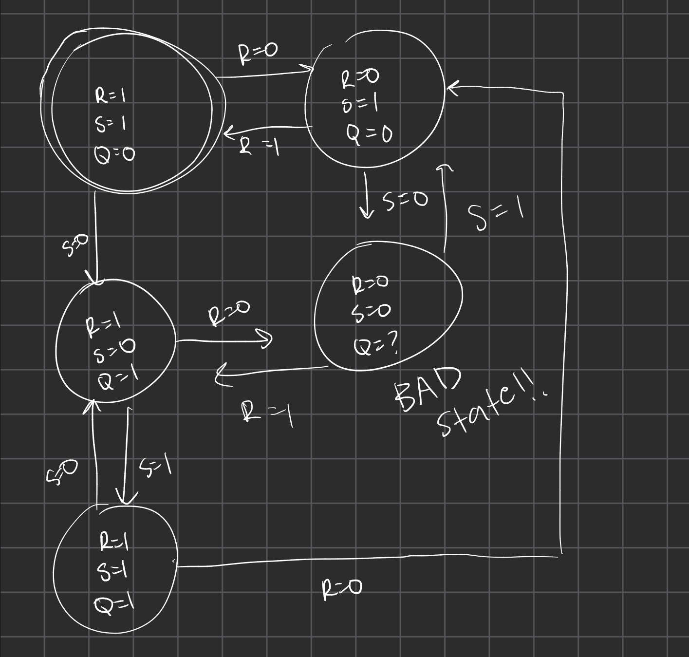
The logic of the RS latch was simple:
- When R = 1, S = 0, which forces Q to 0. This is the reset state.
- When R = 0, S = 1, it forces Q to 1, which is the set state.
- When R and S are both 0, Q holds whatever value it last had. This is the memory behavior that I was explaining earlier.
- When R and S are both equal to 0, there's a problem because they both try to force their output high at the same time, which creates an invalid state. I prevented any transition into this state. (I'll explain this problem a little bit deeper below.)
RS Latch — State Diagram
This part of the project was super cool, but there were two limitations with the RS latch.
- The forbidden state: if R and S are both 0 at the same time, both NAND gates try to force their outputs high simultaneously, which isn't a valid bit because it's not a clean 0 or a clean 1. This means that it has to be explicitly avoided in all instances.
- Manual data memory: the RS latch doesn't have an input that automatically stores a given bit. It has two separate inputs, R and S, and the latch's behavior depends on the relationship between them.
The D latch fixes both issues because it does the RS translation once inside itself. I created this by starting to map the behavior I wanted. If G is 1, then Q should follow D, which is data, and if G is 0, Q should hold the last value, ignoring D entirely. This way it still has the memory behavior of the RS latch. I wired the switches on D and G, and Q to an LED, and then I looked at the hold behavior, and it was exactly what I had expected.
But since the D latch is transparent, the entire time that G = 1, let's say, for a few microseconds, Q tracks D for that entire time window.
So now imagine two D latches are connected in series (latch 1's Q feeds into latch 2's D). Both share the same G clock signal. They both open at the same time. A value could go straight through both latches in one pass, and the second latch would end up not reflecting the previous state, but whatever leaked through from the first latch during the same open window.
For a counter or a processor, that's exactly what causes issues in calculations. Because I needed something that advances exactly one step per clock tick, not something that could let data slip through multiple stages in a single tick. The goal was for me to take the D latch's clean interface, but make the output update at a single instant, and that's where I had moved on to using flip-flops.
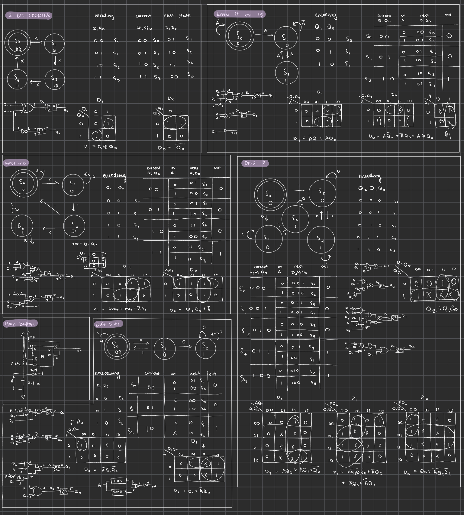
I started experimenting with a 74LS174 hex D-type flip-flop chip. I built a few trivial two-state FSMs, and then I designed more complex FSMs that had pretty cool outputs. My main goal was honestly just to get more familiar with the chip, but it didn't really contribute to the development of the four-bit counter. But, if you're interested, below are the diagrams of the cool circuits I designed. My favorite one was Input 010!
FSM Designs
Tick-Tock
As mentioned above, I switched to a flip-flop. This is just one of the electronic devices that requires a clock pulse signal. So at this point, I permanently wired a 555 timer astable oscillator circuit onto the board. I calculated its output period and frequency by hand and verified that it drove an LED at the expected, visually distinguishable, and slow rate.
After wiring the clock to my breadboard, I started using the counter, which is the 74LS161 chip. This was a synchronous 4-bit binary counter. It has 4 data inputs, 4 outputs, a clock input, and a few control pins with the following behavior:
- Load: When load is high, the counter ignores the data inputs and just increments by 1 on every clock pulse. When load is low, on the next clock pulse, the counter instead loads whatever value is sitting on the data inputs.
- Clear: It's wired high normally. Pulling it low immediately forces all 4 outputs to 0, which is a way to reset the circuit back to its starting state.
- ENABLE P and ENABLE T: These just need to be high to let the counter actually count. I didn't really experiment much with this.
At this point, I wired four switches into data inputs and four LEDs onto the outputs, then I confirmed the behavior that I stated above. Interestingly enough, this is exactly the counter FSM that I'd hand-designed earlier. So, it was now available as a single chip instead of something I had to wire from flip-flops and gates.
At this point, I bought two new chips:
- 74LS181: it's a 4-bit ALU. It's a combinatorial chip which can perform 16 different arithmetic operations and 16 different logic operations on two 4-bit inputs. It also has a carry-in pin, function outputs, and a comparator output that goes high when all four F outputs are high.
- 74LS377: it's an 8-bit register, essentially eight D-type flip-flops sharing one clock and one enable line.
I permanently wired the ALU's function outputs to four of the register's data inputs, and the register's corresponding outputs looped back to the ALU's operand inputs. I also permanently wired the register's output to a row 4 LED indicator circuit, so I could always see the currently stored value.
Without looping register output → ALU's A input, and ALU's output → register's data input, the ALU would just compute A op B once, and the result would disappear the instant that the inputs changed. This is similar to the full adder from earlier. Each clock pulse can take the previously stored value, now sitting on A via feedback, and combine it with the new input B from the switches, then latch the new result back into the register.
Chump!
Part 1 — Data Path
The first goal was to build the compute and store, identical to what I just had explained, but with an input selector and a full memory system.
I wired a selector, the 74LS157 chip, so it picks between two sources, feeding the ALU's B input. The ALU 74LS181 took that selected value plus its own A input feedback, computed the function, and fed its result into the accumulator, the 74LS377. That output was wired to four LEDs and also looped back into the ALU's A input, which is the exact same loop that I just explained above.
I also added an address flip-flop, the 74LS174, and RAM 74S189. The address register holds a memory address, feeds it into the RAM's address pins, and then the RAM's read and write data lines connect it into the same data path so the accumulator can both read from and write to memory.
All nine control inputs were temporarily hardwired using loops of wire to either ground or pull-up resistors. Essentially, I was manually hardcoding one instruction at a time by physically choosing which control lines were high or low. I used the Schmitt trigger pull circuit to single step the clock so I could watch each instruction execute, one step at a time. I was able to do things like load, add, subtract, store, and read, and I was just testing through to see if this was working so far.
Part 2 — Op Codes
I added the 74LS161 as a program counter and wired the ALU's A = B output through a pull-up resistor into a NAND gate alongside the control bit, and then fed that NAND's output into the control counter's load pin. A single control bit decides whether the instruction cares about the accumulator being zero, and if it does, the A = B signal decides whether the program counter increments normally or jumps to a new address. Then I extended the control table to a full 10-bit table covering all 12 instructions, including new ones like “go to” and “if zero.”
Part 3 — Programming the Processor
The final part removed the manual scaffolding entirely. I connected a program ROM, which is a 28C64/28C17-style EEPROM. Its address pins were driven by a program counter, and its 8-bit outputs were split between two 4-bit halves: the high 4 bits as the opcode and the low 4 bits as the embedded constant. I connected a second ROM, which was the control ROM. It took the opcode as its address and, given the output in it, output the 10 control bits that I'd worked out in part 2, replacing the hardwired loops from part 1.
To actually run something, I had to write a short little program using chump instructions, then hand-assemble it, converting each instruction, like add 1, to its 8-bit binary encoding 001000001, where the top 4 bits are the opcode for the add constant and the bottom 4 bits are the constant. I handed that binary off to be programmed into the program ROM. Once it was burned in, the processor ran entirely on its own. The clock ticked, the program counter advanced, and the program ROM handed off instructions. The control ROM translated them into control signals, and the data path executed them.
The Finished Processor
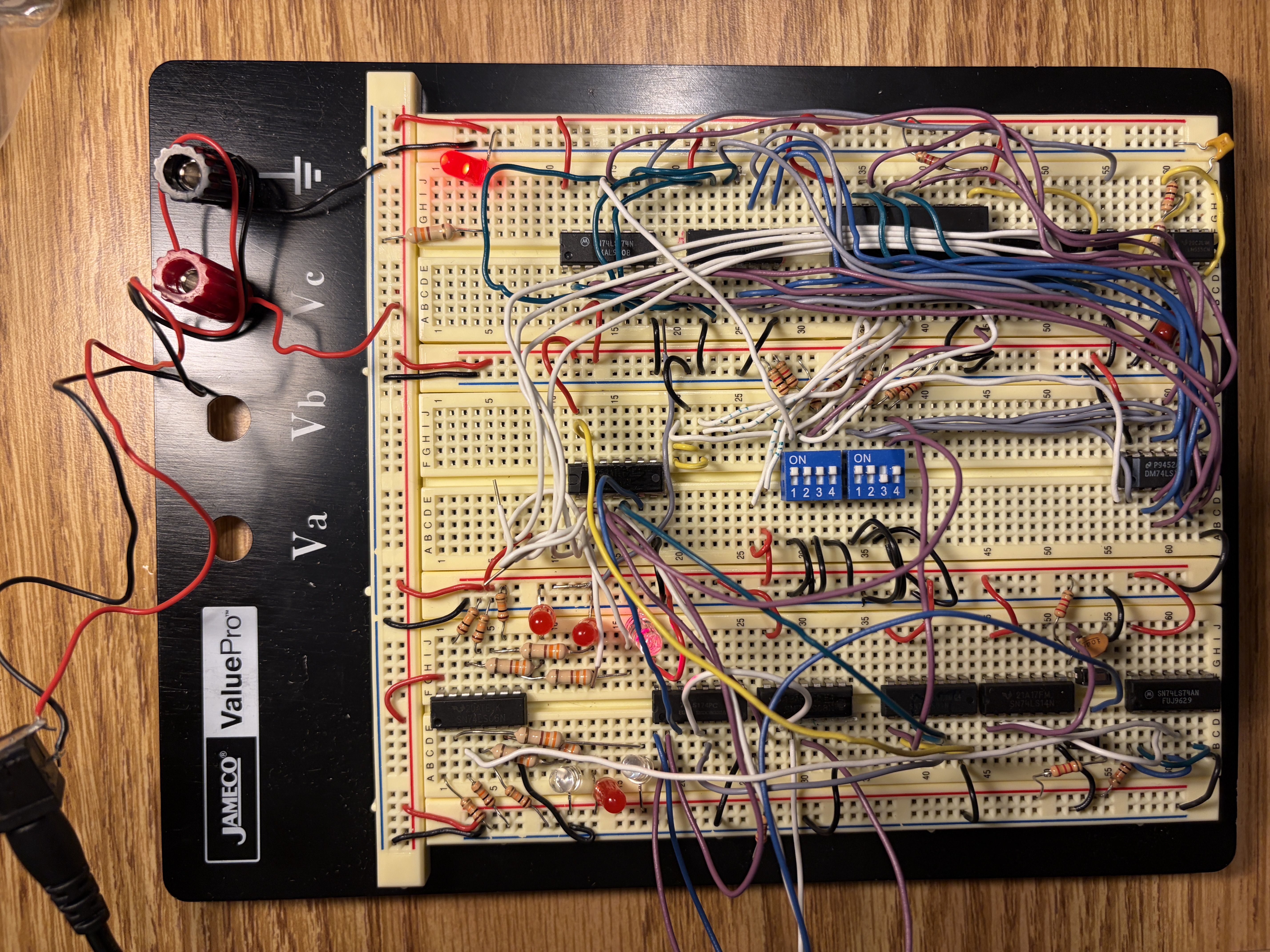
My finished project (: